Typical applications
Control boards, LED support boards, simple power electronics, test fixtures, sensors and IoT modules.
2 Layer PCB Manufacturer
YBCPCB supports 2 layer rigid PCB fabrication for control boards, power boards, IoT modules and general electronics requiring practical manufacturing review.
A 2 layer PCB includes top and bottom copper layers with plated through holes for interconnection. It is commonly selected for straightforward routing, lower density circuits and many prototype builds.
Engineering teams use 2 layer PCB for early validation, industrial interfaces, power boards, sensor modules and control electronics.
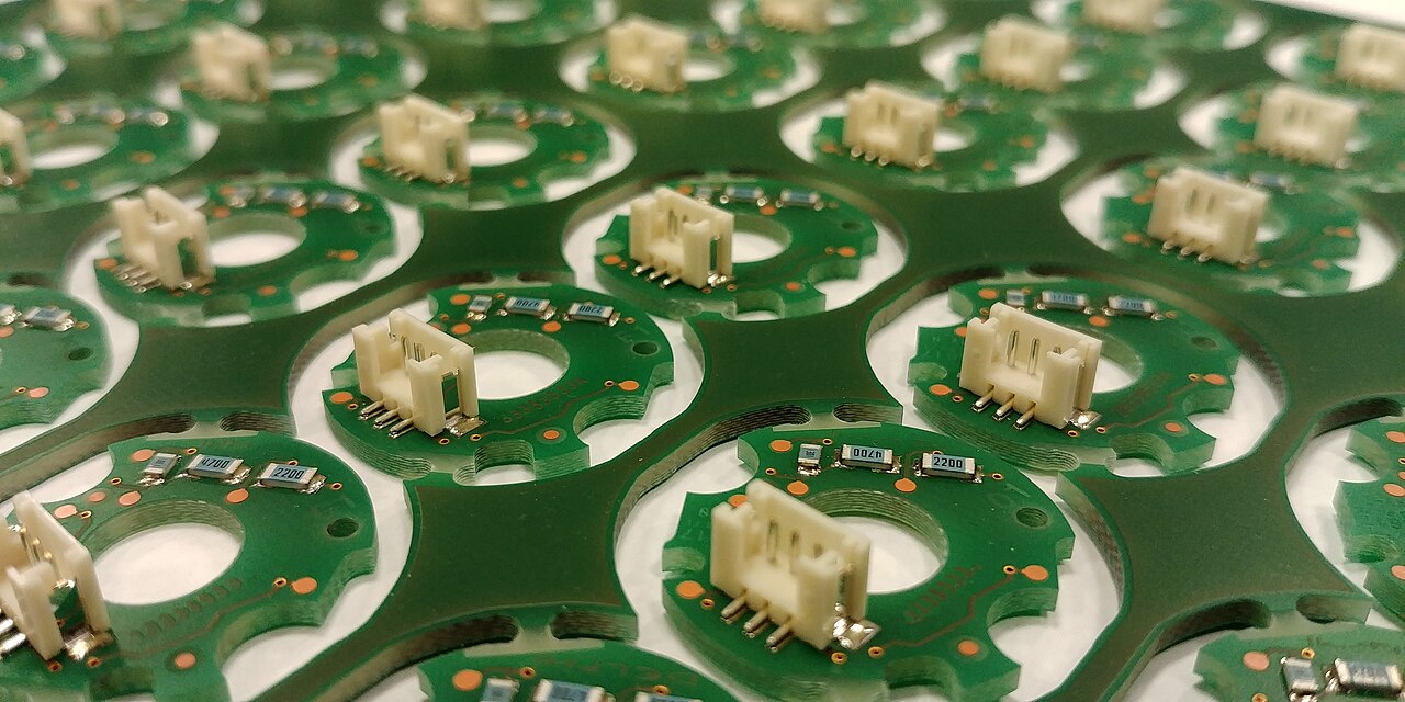
Prepare board outline, drill files, solder mask and surface finish requirements.
| Common specification | Review item | Engineering note |
|---|---|---|
| Copper layers | Top and bottom copper | Check trace width, spacing and copper balance. |
| Material | FR-4 and other materials by review | Select by assembly and operating environment. |
| Finish | HASL, Lead Free HASL, ENIG, OSP | Match pad type and assembly needs. |
| Inspection | AOI, electrical testing and visual inspection | Quality plan follows product requirements. |
Control boards, LED support boards, simple power electronics, test fixtures, sensors and IoT modules.
Simple structure, clear manufacturability and practical transition from engineering sample to production.
Review drill count, copper weight, solder mask clearance, board outline and finish selection.
A 2 layer PCB uses top copper and bottom copper connected through plated holes where required.
Yes. 2 layer PCB is common for prototypes, fixtures and early product validation.
Gerber files, drill files, board outline, material, finish, copper weight and inspection notes are recommended.
Contact engineering with Gerber files, drill data and production notes.