Microvia
Microvias are small vias typically formed by laser drilling. They help route dense components and reduce board area, but require careful pad, plating and stackup review.
HDI PCB Technology
HDI PCB technology supports compact electronic products through microvias, blind vias and high density interconnection structures that require precise manufacturing review.
Microvias are small vias typically formed by laser drilling. They help route dense components and reduce board area, but require careful pad, plating and stackup review.
Blind vias connect an outer layer to one or more internal layers without passing through the full board. They are often used in high density layouts where through holes would consume too much routing space.
HDI structures improve routing density for fine pitch components, compact modules and advanced electronics. Design data should clearly define via structure, layer build-up and critical rules.
HDI PCB is used in medical devices, industrial controllers, IoT devices, automotive electronics, communication modules and portable products where space and signal performance are important.
Important review items include laser drill capability, copper plating, via-in-pad requirements, dielectric thickness, sequential lamination and electrical testing.
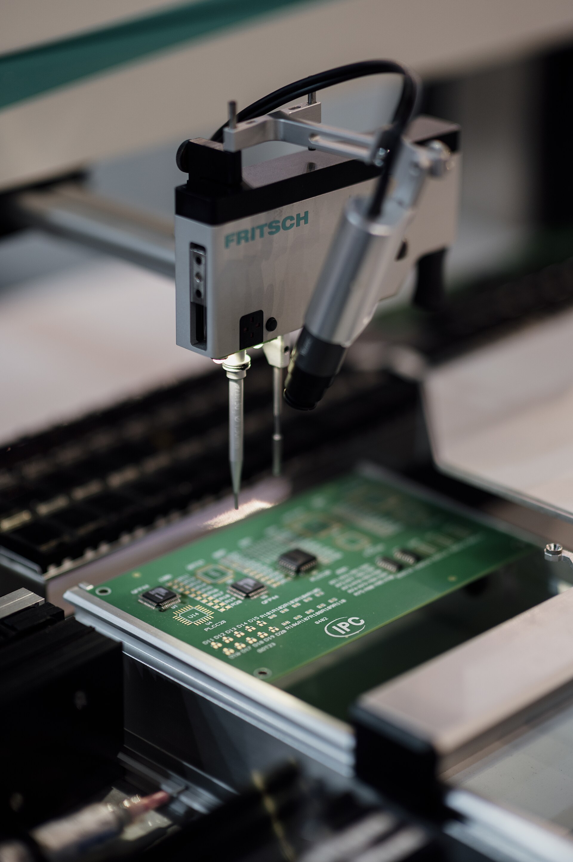
YBCPCB reviews PCB files, material requirements, stackup notes and inspection needs before production planning.
Microvias are small vias typically formed by laser drilling. They help route dense components and reduce board area, but require careful pad, plating and stackup review.
Blind vias connect an outer layer to one or more internal layers without passing through the full board. They are often used in high density layouts where through holes would consume too much routing space.
HDI structures improve routing density for fine pitch components, compact modules and advanced electronics. Design data should clearly define via structure, layer build-up and critical rules.
Send files, stackup notes and manufacturing requirements for technical review.