Layer stackup
A multilayer PCB stackup defines copper layers, dielectric thickness, prepreg, core material, ground planes and power planes. Early stackup confirmation helps control impedance, board thickness and drilling structure.
Multilayer PCB Engineering
Multilayer PCB design requires careful stackup planning, material selection and manufacturing rule review to support signal quality, power delivery and production stability.
A multilayer PCB stackup defines copper layers, dielectric thickness, prepreg, core material, ground planes and power planes. Early stackup confirmation helps control impedance, board thickness and drilling structure.
FR4, High Tg and halogen-free materials are selected according to thermal performance, reliability, compliance and application environment. High layer count designs often require closer material and lamination review.
Controlled impedance, return paths, plane reference, via transitions and trace spacing influence high-speed performance. Designers should provide impedance requirements and critical net information when available.
Manufacturing review should cover minimum trace and spacing, hole size, annular ring, copper balance, solder mask clearance, panelization needs and final inspection requirements.
Multilayer PCB is common in industrial electronics, medical equipment, automotive control, IoT gateways, power electronics and communication systems.
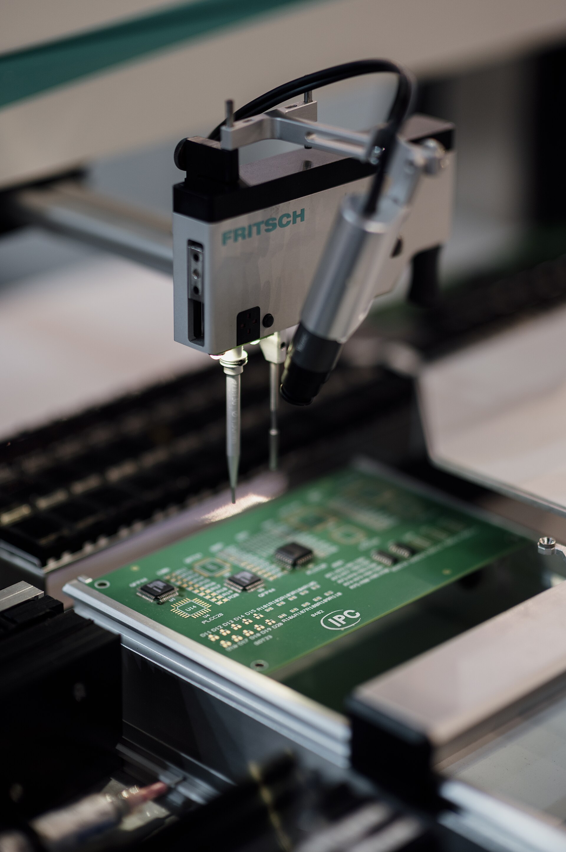
YBCPCB reviews PCB files, material requirements, stackup notes and inspection needs before production planning.
A multilayer PCB stackup defines copper layers, dielectric thickness, prepreg, core material, ground planes and power planes. Early stackup confirmation helps control impedance, board thickness and drilling structure.
FR4, High Tg and halogen-free materials are selected according to thermal performance, reliability, compliance and application environment. High layer count designs often require closer material and lamination review.
Controlled impedance, return paths, plane reference, via transitions and trace spacing influence high-speed performance. Designers should provide impedance requirements and critical net information when available.
Send files, stackup notes and manufacturing requirements for technical review.