Manufacturing Tolerances
PCB manufacturing tolerances guide for design review.
Tolerances affect drilling, line width, spacing, registration, routing and final inspection. Clear notes help prevent ambiguity before production.
Manufacturing tolerance topics
PCB tolerance planning should consider finished board outline, plated hole size, non-plated holes, slot geometry, trace width, spacing, solder mask registration and layer-to-layer registration.
Inspection planning
Critical dimensions should be called out in fabrication drawings or notes. Inspection expectations should match the product application and customer requirements.
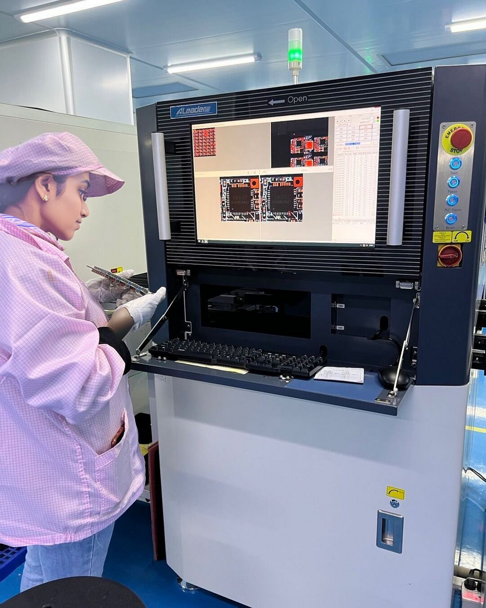
Inspection focus
AOI and electrical testing support consistent quality review.
| Tolerance area | Review focus | Buyer note |
|---|---|---|
| Hole tolerance | Finished hole size and plating requirement | Confirm connector and fastener requirements. |
| Line width | Copper weight, process capability and spacing | High copper needs early review. |
| Registration | Layer alignment and solder mask alignment | Important for fine pitch and dense layouts. |
| Board outline | Routing, slots, cutouts and mechanical fit | Provide clear outline and drawing notes. |
Review tolerance requirements before production.
Send fabrication notes, drawings and critical dimensions for engineering review.