Quality requirements
Quality planning may include AOI, electrical testing, visual inspection, dimensional checks, packing review and project-specific documentation.
PCB Case Study Structure
Prepared as a no-customer-name template for explaining application background, PCB requirements, manufacturing considerations, quality requirements and production solution.
IoT devices often combine compact layouts, wireless modules, sensors, power management and enclosure constraints that require careful PCB manufacturability review.
Common requirements include fine line routing, multilayer or HDI PCB review, ENIG surface finish for dense pads, material stability and clear testing criteria.
Engineering review should confirm Gerber files, drill data, board outline, stackup, material, surface finish, solder mask, testing route and final documentation expectations before production release.
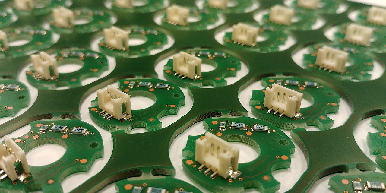
The structure helps buyers connect application requirements with practical PCB manufacturing decisions.
Quality planning may include AOI, electrical testing, visual inspection, dimensional checks, packing review and project-specific documentation.
The production solution emphasizes stackup review, impedance-sensitive area checks, pad finish selection, electrical test planning and communication of assembly-related notes.
Capability review connects PCB type, layer count, material, copper weight, finish and testing method with the final application.
Send files and application notes for engineering review.